 adhesion The downside of this method is the mechanical stability of the thin-film roof, which is a limitation in some applications. The fabrication of those devices requires a previous step of micro-patterning. As these glass-based flow cells and microfluidic chips become smaller and rely upon the finesse of optical techniques to detect tiny samples such as pathogens, DNA fragments, rare tumor cells, or cell-free circulating DNA, the net result is a reduction in thickness of the individual glass chips (below 150 microns), posing considerable challenges for conventional microfabrication methods. At the Berkeley Space Sciences Laboratory, we are working to further expand this technology by developing analytical instruments to chemically explore our solar system.
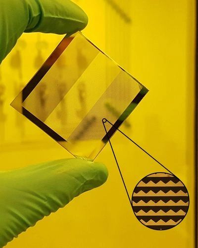
5, p. 1307, May 2011. The design corresponds, in most of the cases, to micrometric features. 6162. This set of values minimizes the losses of light transmittance during microscope observations. Los resultados corresponden a la realizacin de PPP en portaobjetos de vidrio y compuesto por puntos laterales de 2m hechos de aluminio con un grosor de 30nm. In order to confront the previous mentioned challenges, the patterning of cell-culture dishes presented in this work was done using micro-technology procedures, specifically through an adapted lift-off process. This manuscript provides detailed information on microfabrication technology for the production of high-quality glass microfluidic chips in compliance with industrial standards and space flight instrumentation quality control. The procedure of photolithography onto the mentioned substrate is depicted in Fig. As a result, particles of aluminum land everywhere and create a continuous layer. This article presents the procedure of microfabrication of those PPP, indicating the obtained results as well as the issues encountered. The combination of this resist and an appropriate exposure time and dose (45 mJ/cm2) during development ensure a pattern that is small and reliable enough for accurate ROI localization (by suitable image processing techniques). Exposure is done through the negative mask. 2, no. Borosilicate or its tempered trademarked version "PYREX" is widely used in MEMs and microfluidic diagnostic applications. Also, we acknowledge the financial support given by Instituto Tecnolgico Metropolitano (Medellin-Colombia), and by Institute FEMTO-ST (Besancon- France), under the project number P15201. It is important to use a considerable development time (normally to obtain 30% of over-developing) that avoid the presence of photo-resist in the forming undercuts. Reversal bake is done on a hot plate for 1 min at a temperature of 130 C. 2012 Biomicrofluidics, 2022 Darwin Microfluidics. Substrate is immersed in a liquid made of a powerful photoresist solvent that is chemically inert on glass and metal. La microfabricacin presentada se basa en una tcnica conocida como lift-off que, tras el ajuste de parmetros, permite la obtencin de PPP cumpliendo los dos requisitos anteriormente mencionados. It also aids automatic and highly accurate position retrieval when the patterned slides are placed on Petri dishes or other devices supporting the cell cultures. En estos casos, aparecen dos desafos principales: 1) Las perturbaciones en la transmisin de la luz deben permanecer mnimas para mantener la alta calidad de observacin del objeto de inters bajo el microscopio. The methodological protocol provided in this paper includes the scope of each step of the manufacturing process, materials and technologies recommended and the specific challenges that often confront the process developer. You can download the paper by clicking the button above. [10] D. B. Boyton, Position encoder using statistically biased pseudorandom sequence. 2004. MicroChemicals GmbH, 2007. Once the dissolved photoresist is stripped out from substrate, the aluminum layer over it is lifted-off, while the metal deposited directly on the substrate remains. 2.5:1), an associated taper angle of 22 degrees (or more), and most important, this technique is challenged by the handling of thin glass slides due to the high pressure flow of the particles and carrier fluid. [1] R. Ramji, N. T. Khan, A. Muoz-Rojas, and K. Miller-Jensen, Pop-slide patterning: rapid fabrication of microstructured PDMS gasket slides for biological applications, RSC Adv., vol. Resumen:
2, p. 278, Jan. 2017. In the case of sputtering, the substrate and a target (the material to be deposited) are placed in a vacuum chamber. Over the years, CO2 lasers have been used for drilling and dicing of thick glass sheets and slides, limited by the hole diameter (recently as small as 50 -70 microns), but more importantly by the thermal damage and debris generation resulting from a variety of industrial and laboratory processes. Commercial UV lamps are already equipped with a specific device to perform this adjustment automatically. 172 rue de CharonneBtiment B1, 1er tageParis, France. The fourth step consists in the flood exposure of photoresist with dose of 190 mJ/cm.. For this exposure we do not use any mask. 248, pp. Enter the email address you signed up with and we'll email you a reset link. All etch processes require a conformal mask to define the hole pattern, creating additional process steps. 6. It is quite simple and gives good results. Jabil Scores MedAccredPlastics Injection MoldingAccreditation, How Medtronic Is Creating Equal Supplier Opportunity. This problem was solved by adjusting the exposure dose. In these cases, the micrometric features allow the absolute localization of the observed areas with diverse ranges of resolution and accuracy with respect to the whole substrate. This consists in transferring a pre-defined design onto the substrate by means of techniques such as mask UV-lithography, mask-less lithography systems such as laser-direct-writing-lithography, and inkjet printing [5], [6]. The sequence of image-reversal resist processing as a negative photoresist. HF etching is an isotropic process resulting in the holes or channels being etched near the tops of the features nearly twice as wide as deep. Published by Elsevier B.V. https://doi.org/10.1016/j.mex.2020.101043. In future works it will be important to consider the use of other metals for the PPP. We willcompare3microfabrication processes that make it possible to transform these materials into microfluidic devices: surface micromachining, buried channel techniques and bulk micromachining. During the evaporation process, the substrate is placed in a high vacuum chamber at room temperature. For PDMS preparation, we used a standard process that implies the use of the PDMS itself together with a curing agent, as presented in the following [18]: 1. After exposure, the photoresist is subjected to reversal bake. This is known as patterning, which is a technique that can also be used in transferring specific designs that allows region of interest (ROI) recovery under the microscope. Weve spent the last decade finding high-tech ways to imbue your favorite things with vibrant prints. This causes material to be sputtered off the target and condense on the substrate. The idea is to represent present dots by aluminum covered areas. 4, no. Los portaobjetos de microscopio se utilizan ampliamente como sustratos base in situ para la realizacin de diversos sistemas o elementos microfabricados. The time specification given refers to the development start. Therefore, the optimum dose of the first exposure depends on the desired undercut and the minimum lateral feature sizes [16]. photomask photomasks services manufacturing lithography <10 um/min).
The advanced development of faster, cleaner glass cutting processes, especially with smaller and thinner glass microfluidic chips and MEMs devices, opens up opportunities for laser microfabrication to be an attractive, cost-effective high volume manufacturing process. En estos casos, aparecen dos desafos principales: 1) Las perturbaciones en la transmisin de la luz deben permanecer mnimas para mantener la alta calidad de observacin del objeto de inters bajo el microscopio. Centrifugate the substrate with the PDMS mixture for 40 secs to obtain a uniform PDM S layer on the substrate. For this, three types of photoresist can be used: positive, negative and image reversal. 3.
 Bulk micromachining, on the other hand, cannot offer such channel height control due to spatial variations in etching speed. Copyright 2022 Elsevier B.V. or its licensors or contributors. It is possible to see the pattern size (around 2m) with a period of 4m. For ROI recovery, different approaches have been proposed, most of them corresponding to alpha-numeric patterns that, once embedded in Ptri-dishes or microscopes-slides, offer a visual way for ROI positioning. All Rights Reserved, Product successfully added to your Shopping Cart. Different from the mentioned approaches, our method also allows orientation measurement. As an example, we can reference the pattern presented by Dominic et al. Creative Commons Attribution 4.0 International. In this method, micro- and nanofluidic channels are formed by removing excess material from a wafer and bonding or adhering it to another wafer to encapsulate the channels. 81, pp. Our team keeps you informed of the latest news at Darwin Microfluidics. Informa Markets, a trading division of Informa PLC. In our case, we proposed to transfer specific pseudo-periodic patterns (PPP) onto the ground side of Ptri-dishes. [17] M. J. Madou, Manufacturing techniques for microfabrication and nanotechnology, 1st ed., vol. All rights reserved. The use of any of the above-mentioned techniques depends on the capacities of the micro-technological facility, being mask-less lithography a more flexible technology allowing the fabrication of shapes with a minimum feature size as small as a few nanometers [7], [8]. The presented microfabrication is based in a technique known as lift-off, which after parameter adjustment, allows the obtaining of PPP fulfilling the two previously mentioned requirements. Opt. Although those types of patterning are nowadays commercialized and used by many biologists, the allowed performances are coarse and constitute a major limiting factor for high-accurate analysis of cellular events. Particularly interesting are so-called non-linear processes where the short pulses are employed to form very limited channels of ionized gas within the target material. Esos patrones estn embebidos en placas de Ptri para permitir la recuperacin absoluta y de alta precisin de una ROI, al igual que su orientacin. A series of cross-sections of an image reversal resist in different stages of development. 5, no. Indeed, the thickness of the sacrificial layer that corresponds to the final height of the channel can easily be controlled to the nearest nanometre. Aside from mechanical CNC drilling and milling of large features (typically less than 500 microns), abrasive machining is also a common technique to drill holes, employing a contact or conformal mask (i.e. The procedure consisted in patterning a glass microscope cover-slip, which was then inserted in a plastic Ptri dish. Web page addresses and e-mail addresses turn into links automatically. The introduction of ultrafast lasers, whose pulse duration (the amount of time the laser flash exists in time, typically measured in picoseconds (10-12) or femtoseconds (10-15)) is six to nine orders of magnitude shorter than typical CO2 laser pulses has opened up exciting opportunities for the fabrication of thin glass microfluidic chips. exchanger applied rtds 1, pp. 3).
For such purposes, the micro-fabrication process consists in transferring a pre-defined design onto the substrate made of a glass microscope slide. 2.
 Extracted from Iliescu et al.
 Place the substrate in an oven at 80C for 8 hours to soft bake the PDMS mixture. 6582, Jan. 2010. One must notice a negative profile of the photoresist's walls. Keywords: Microtechnology, lift-off process, pseudo-periodic patterns, glass microscope slides, micropatterning. 2) The pattern-size should then be small enough but, however, larger than the diffraction limit to be observable satisfactorily for positioning purposes. MD+DI Online is part of the Informa Markets Division of Informa PLC. [12] M. J. Yao, Method of printing location markings on surfaces for microscopic research. 2013. Those features form the pattern that is desired to be reproduced by photolithography, in our case a PPP. The obtained patterned cover-slips were embedded in Ptri dishes as well as in well plates. Ultrafast lasers can also cut thin glass (thickness of less than100 microns) without the inherent process drawback of particle blasting or ultrasonic drilling. Prefered process options are shown in bold. The results report on PPP realized on glass microscope slides and composed by 2m side dots made of aluminum with a thickness of 30nm. 2020 The Authors. 1. They're enabling further advances in MEMS and microfluidic diagnostic applications. That means: We can print whatever you need on a massive variety of mediums. Micromanufacturing in Fused Silica via Femtosecond Laser Irradiation Followed by Gas-Phase Chemical Etching, Selective iterative etching of fused silica with gaseous hydrofluoric acid, Manufacturing of microchannels in soda-lime glass by femtosecond laser and chemical etching, Fabrication of large-volume microfluidic chamber embedded in glass using three-dimensional femtosecond laser micromachining, Shape control of microchannels fabricated in fused silica by femtosecond laser irradiation and chemical etching, Dr. Krishna Chaitanya V, Assistant Professor, Physics, SSSIHL, Femtosecond laser internal manufacturing of three-dimensional microstructure devices, CO2 laser polishing of microfluidic channels fabricated by femtosecond laser assisted carving, Fabrication of microchannels in glass using focused femtosecond laser radiation and selective chemical etching, Femtosecond laser fabricated monolithic chip for optical trapping and stretching of single cells, Femtosecond laser machining of multi-depth microchannel networks onto silicon, Low-cost microfluidics on commercial grade poly(methyl methacrylate) (PMMA) using deep-UV patterning, Organic random laser in an optofluidic chip fabricated by femtosecond laser, Femtosecond laser fabrication of microfluidic channels for organic photonic devices, Integrating photonic and microfluidic structures on a device fabricated using proton beam writing, Fabrication of a glass capillary electrophoresis microchip with integrated electrodes, Deep trenches fabricated by laser-induced backside wet etching for guiding light, Fabrication of Large Scale Nanofocusing Device Based on Negative Refraction Index Photonic Crystals, Femtosecond micro- and nano-machining of materials for microfluidic applications, Crack-free direct-writing on glass using a low-power UV laser in the manufacture of a microfluidic chip, Glass optical waveguides: a review of fabrication techniques, Manufacture of microfluidic glass chips by deep plasma etching, femtosecond laser ablation, and anodic bonding, Effect of process parameters in nanosecond pulsed laser micromachining of PMMA-based microchannels at near-infrared and ultraviolet wavelengths, Inscription and characterization of micro-structures in silicate, FOTURANTM and tellurite glasses by femtosecond laser direct writing, Laser Beam MicroMachining (LBMM) -A review, Microfluidic devices for small-angle neutron scattering 1,
[13] M. Wrenn and D. Soenksen, Systems and methods for tracking a slide using a composite barcode label. 2016. Glass microscopes slides are widely used as in situ base-substrates carrying diverse micro-fabricated systems or elements. The exposure dose strongly impacts the lineal resist profile. 4360.
The thickness of the aluminum in the PPPs ranged from 30 nm to 100 nm. Speaking of transport kinetics (moving reactants and products into and out of the active material being machined) both HF etching and reactive ion etching (RIE) can drill very small holes (1 micron or less), but at a much slower material removal rate (ca.
[4] N. Nagarajan, K. Hung, and P. Zorlutuna, Protein Micropatterning Techniques for Tissue Engineering and Stem Cell Research, in Cell and Material Interface: Advances in Tissue Engineering, Biosensor, Implant, and Imaging Technologies, vol. Absent dots and background correspond to the transparent substrate itself. The undercut forms in the last stage of development, according to the development time, are presented in Fig. Microdevices, vol. In those cases, two main challenges appear: 1) Disturbances in light transmission should remain minimum to keep the high quality of observation of the object of interest under the microscope. In all the cases, the photoresist-covered substrate is exposed to UV-light through a mask. The presented microfabrication is based in a technique known as lift-off, which after parameter adjustment, allows the obtaining of PPP fulfilling the two previously mentioned requirements. En este artculo presentamos los procedimientos involucrados en la microfabricacin de Patrones Pseudo-Peridicos (PPP) los cuales encriptan la posicin absoluta de un rea extendida. This requires micron-scale lithography and a high aspect-ratio DRIE. We are dedicated team of designers and printmakers. Glenn Ogura is the SVP Market Development atResonetics(Nashua, NH). [7] K. Boolchandani and B. Sarita, A Review Paper on Nanotechnology Applications and Concepts, in IJIRST || National Conference on Innovations in Micro-electronics, Signal Processing and Communication Technologies (V-IMPACT-2016), 2016, pp.
The mask was designed and elaborated in a chromium-covered silica glass slide.
[8] A. In the second step, photoresist is exposed to UV light with dose of 45 mJ/cm.. However, it was indeed with glass and silicon that the first microfluidic devices were created, i.e. This causes the photoresist's sidewalls with negative profile to remain clear (Fig. Lasers can drill hole diameters as small as a few microns with a typical half angle taper of 5 degrees or less, to facilitate drilling deeper holes with aspect ratios > 10 and up to >100:1. [18] Elveflow, How to do PDMS lithography replication from a su-8 mold: The PDMS lithography replication process: tips and tricks, The SU-8 mold fabrication process: tips and tricks. By continuing you agree to the use of cookies. Plasma is generated in a side gas source in the chamber, and the ion bombardment is directed towards the target. 2) El tamao del patrn debe ser entonces suficientemente pequeo, pero, sin embargo, mayor que el lmite de difraccin para ser observable satisfactoriamente para propsitos de posicionamiento. In buried channel technology, the idea is to create a deep access trench by direct anisotropic deep reactive ion etching (DRIE) of silicon. The side walls are passivated by chemical vapour deposition (CVD), and a circular channel is then isotropically etched, with the bottom of the access trench centrally located [Paick SJ et al. The surface micromachining technique consists of the use of a sacrificial layer which is shaped to define the desired fluid channels, then a structural layer is deposited and finally the sacrificial layer is etched. In our case, for PPP patterning, we used the last mentioned photoresist. During development, areas exposed first remain whereas unexposed are stripped. How Lasers Are Boosting Glass Microfabrication, An AI System Catches Sepsis Hours Earlier than Traditional Methods, Subtle Software Changes Delay Dexcoms G7 FDA Nod, Theranos Whistleblower to Kenyote BIOMEDevice Boston, Qosina Introduces AseptiQuik STC Connectors & More Supplier News, New Partnership Will Help ID At-Risk Cardiology Patients Using AI, Acutus Has a Wider Reach for 3D Imaging and Mapping Catheter, Allowed HTML tags:
. Given their uses and its physical properties, microscope slides are used nowadays as base-substrates for the development of microfabrication-based devices such as microfluidics and Lab-on-a-Chip [1][4]. Para estos fines, el proceso de microfabricacin consiste en transferir un diseo predefinido sobre el sustrato correspondiente a una lmina de vidrio utilizada como portaobjetos de microscopio. In the case of a positive profile, the sidewalls would be slightly covered.
We calculated a light budget of 85%, for the aluminum and PPP configuration used in this work. 109146. In those cases where it is acceptable for the application, the final performance of the device is limited due to the roughness and potential reactivity of the resulting surfaces. Should Medtech Get First Dibs on Semiconductors? The microfabrication of glass-based microfluidic chips requires drilling, cutting and etching to create features such as entry via holes, micro-channels or flow cells. Microfabricated glass microfluidic and Capillary Electrophoresis (CE) devices have been utilized in a wide variety of applications over the past thirty years. The processing of the PPP image allows to measure in a precise way the position of the cell-culture under observation as reported elsewhere [15].
This image reversal type photoresist was used in a negative way over the glass-slides substrates. 374379. Deep reactive ion etching (DRIE) has a much higher aspect ratio (50:1) but is constrained by a slow etch rate of ~250-600 nm per minute that translates into higher costs due to lower throughput and more expensive vacuum and gas handling systems. Search for medtech contract manufacturers on our Qmed Directory,the world's only directory of pre-qualified suppliers to the medical device and in vitro diagnostics industry. Nevertheless, the thickness of the metal layer on them is negligible. Abstract: Los portaobjetos de microscopio se utilizan ampliamente como sustratos base in situ para la realizacin de diversos sistemas o elementos microfabricados. 4 for the photoresist patterning on coverslip glasses using image reversal photoresist as a negative one. The chamber has a crucible, placed under the substrate, that contains the material to be depositedaluminum, in our case. This is the case of applications where region of interest (ROI) recovery is needed either for absolute alignment or for cell-migration quantification and follow-up. In general, the lift-off method comprehends the following steps: photolithography, metallization, resist stripping and metal lift-off. Copyright 2022. We present robust and rigorous manufacturing and quality control procedures that will assist other researchers in achieving the highest possible quality glass microdevices using the latest apparatus in a routine and reliable fashion. Surface micromachining is particularly interesting for the fabrication of nano-channels. We also write some nice reviews and tools to guide you through the vast world of microfluidics! High exposure doses homogeneously expose the resist film towards the substrate, the resist profile shows almost no undercut.